Precision Inspection Systems for Zero-Defect Semiconductor Manufacturing
In semiconductor manufacturing, quality is measured in microns and errors are not recoverable. Even the smallest defect can lead to device failure, yield loss, and costly scrap. Lucid Imaging delivers advanced machine vision inspection systems designed to ensure maximum yield, process stability, and defect-free semiconductor production.
Semiconductor manufacturing is one of the most precision-driven industrial processes, involving multiple stages such as wafer fabrication, patterning, inspection, dicing, and packaging. Each step introduces potential defects that must be detected early to protect yield and reliability.
As device geometries continue to shrink and production volumes increase, manual inspection becomes impractical. Automated machine vision inspection plays a critical role in maintaining process control, defect visibility, and consistent quality throughout the semiconductor value chain.
Quality Challenges
Key Quality Challenges in the Semiconductor Industry
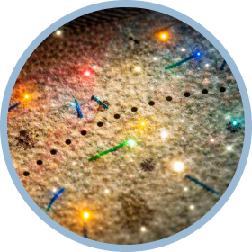
Micro Surface Defects
Detect fine wafer-level imperfections.
Pattern Variations
Identify process deviations accurately.
Contamination & Scratches
Spot particles and surface damage early.
Handling Defects
Capture issues from transfer and processing.
Packaging Errors
Verify correct marking and packaging quality.
Late-Stage Yield Loss
Prevent losses through early detection.
Defect Trend Visibility
Gain insights across production processes.
How It WOrks
Why Automated Inspection is Critical
Semiconductor fabs demand absolute precision and repeatability. Automated inspection systems provide:
01
High-Resolution Detection
Capture micro and sub-micron defects with precision.
02
Full-Speed 100% Inspection
Inspect every item without reducing production speed.
03
Consistent Quality Decisions
Ensure objective and repeatable inspection results.
04
Early Defect Identification
Detect issues early to improve overall yield.
05
Actionable Process Insights
Use data and analytics for continuous improvement.
End-to-End Coverage
Scope of Inspection
Lucid Imaging’s semiconductor inspection systems cover:
Wafer Surface Defects
Detect contamination and surface flaws.
Pattern Integrity
Verify alignment and feature accuracy.
Damage Detection
Identify scratches, cracks, and handling issues.
Die & Package Inspection
Ensure surface quality at all stages.
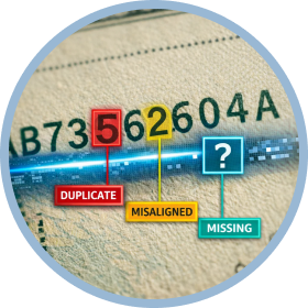
Marking Verification
Validate laser codes and identification marks.
Traceability Control
Track lot, batch, and process data.
Inspection Analytics
Log data for monitoring and improvement.
OUR SOLUTIONS
Lucid Imaging Solutions for the Semiconductor Industry
Lucid Imaging offers inspection solutions tailored for semiconductor manufacturing and packaging environments:
FOUP Inspection
Provide continuous defect detection across high-speed paper webs.